electronics design
-----------------------------------------------------------------------
steps:
this week's assignment was to redraw the echo-hello-world circuit board and add a button and LED. The steps are listed below:
- 1. redraw the echo-hello-world board with Eagle or KiCAD (i chose Eagle) in the schematic mode adding an LED and button.
- 2. lay out the board in board mode after setting the design rules to the given design fab rules such that the thickness of the traces for milling are sufficient.
- 3. draw the outline of the board on a different layer.
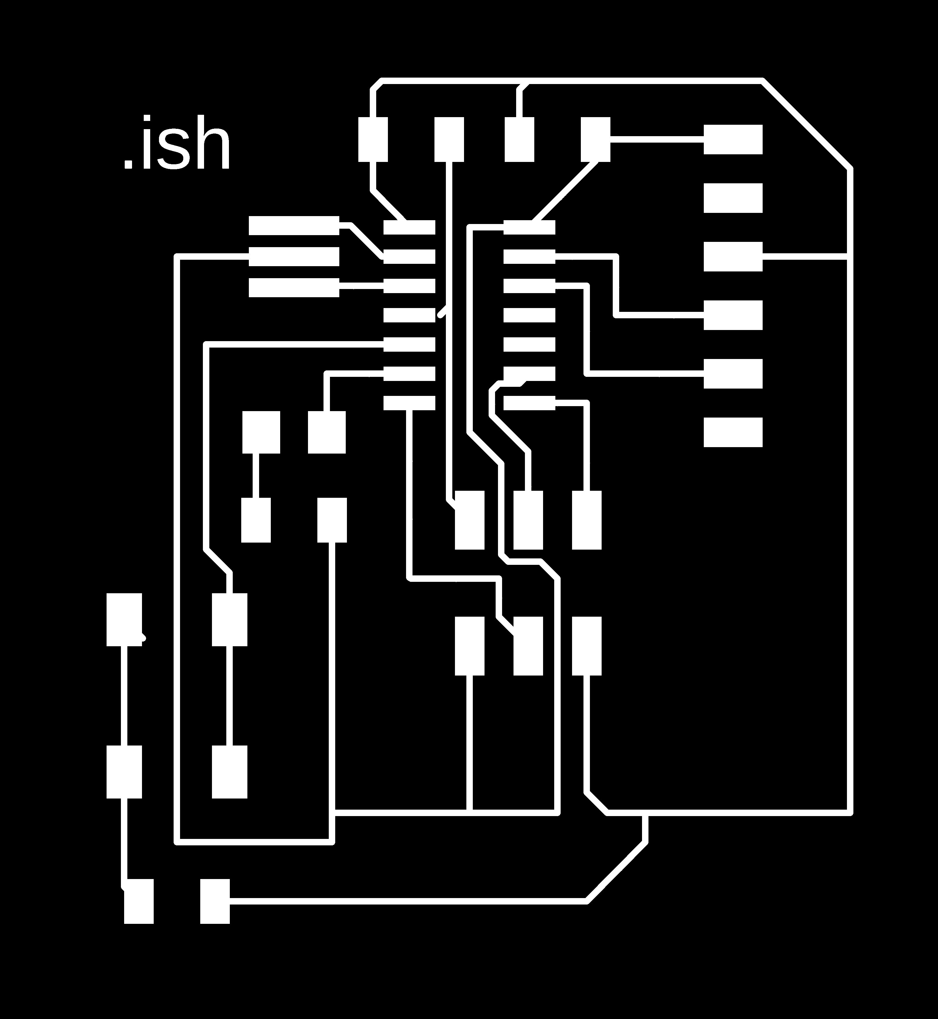
- 4. export the top layer with the circuit board layout and the polygon outline of the board layer as two seperate .png images ensuring that they are the correct size.
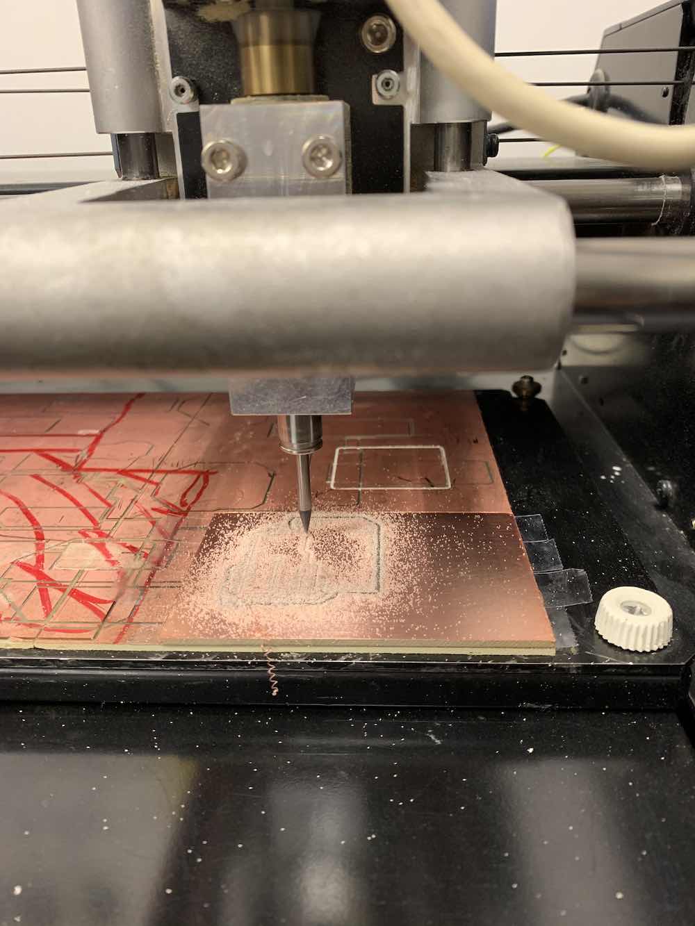
- 5. mill the baords using a Roland machine.
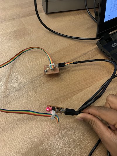
- 6. solder each of the components.
- 7. program the board using the USBTiny programmer we made two weeks agao and uploading the echo-hello-world code.
this week was really difficult for me, because it was the first time that i had to use Eagle to design a board and debug, since there were many problems that came up. i learned a lot of lessons during the process that will be really useful for future circuit boards that i have to make for this class. below is a more in depth look at each step from above.

step 1
eagle: figuring out Eagle was my first challenge of the week. i had never used it, so it was particularly difficult to figure out the shortcuts and methods of making the schematics process easier. Eagle is a free Autodesk software specifically for electronic circuit design.
import Fab Library: one of the first steps to do after opening eagle is to import the fab library of components (available on the class site repo). this library will have all the components available in the fab lab, which is much easier than parsing through the hundreds of components that Eagle provides you with. after importing, the trick is to right click on all the other libraries and ensure they are marked as "use none" and a grey dot is next to the parts. "use all" of the fab library and a green dot should be displayed next to all the parts.
schematic design: this took me a while to figure out. the way to add parts is through the left menu button "add part." then i tried to attach the corresponding names with matching ones on other parts
- the parts we will need are:
- (1) XTAL1 20 MHz is a resonator, which is listed under XTAL_RESONATOR
- (2) RESONATOR R1 10k is a resistor, which is listed under R
- (1) RESONATOR R1 1k is a resistor, which is listed under R
- (1) C1 1uF is a capictor, which is listed under CAP
- (1) t44 is a microchip, which is listed under UC_ATTiNY44
- (1) J1 iSP is a microcontroller, which is listed under AVRiSPSMD
- (1) J2 FTDi is a microcontroller, which is listed under FTDi-SMD-HEADER
- (1) LED is a led light, which is listed under LED
i didn't learn the tricks of Eagle until too late going to the EECS office hours to get my board checked before milling it. in the future, i'll be making sure to label and name my wires to make sure they don't get jumbled in the process and that will appear on the board.

step 2:
laying out the board was a big puzzle for me. what i found the most useful was to look at neil's hello-world board and doing a similar layout and then add the button and led in the space that is free. also i imported the design rules from the site repo to my board to make sure my board will be milled correctly.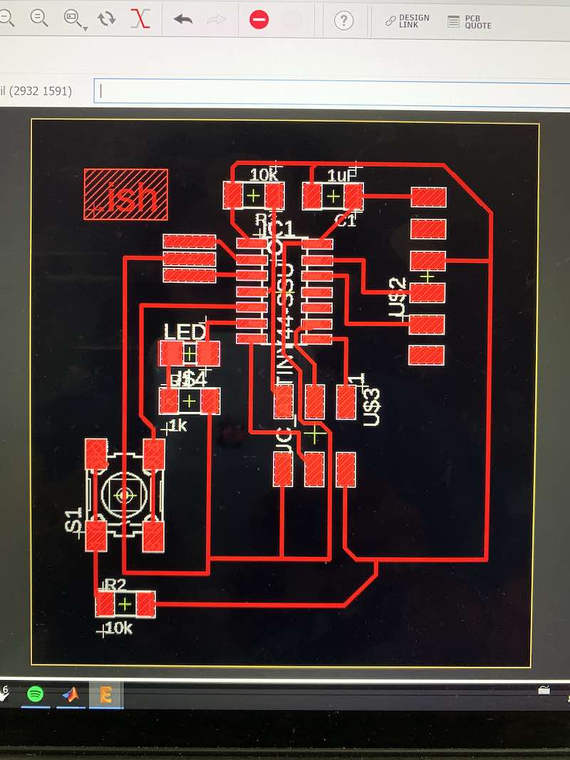
step 3:
for the outline of the board, i clicked on a different layer, and used the polygon tool to draw the shape of my board.

step 4:
i exported the top layer with the circuit board layout and the polygon outline of the board layer as two seperate .png images ensuring that they are the correct size (1000 dpi). to do this i had to "disp none" and then "disp top" for the traces layer and then "disp none" and "disp mill" for the outline layer. when i went to mill the board, i soon found that i had the incorrect dpi for my screen size to convert to the mods program, i should have exported the .png images as 2000 dpi.
step 5:
i milled my circuit board the same method that we milled boards two weeks ago. there were no problems or anything unexpected at this step.
step 6:
soldering the components were fairly straightforward for me as well. i enjoyed doing it two weeks ago and felt the process to be relaxing, so i really enjoyed this step. if the board and schematic were labeled correctly with the parts listed above, then getting the parts were not a problem for me.

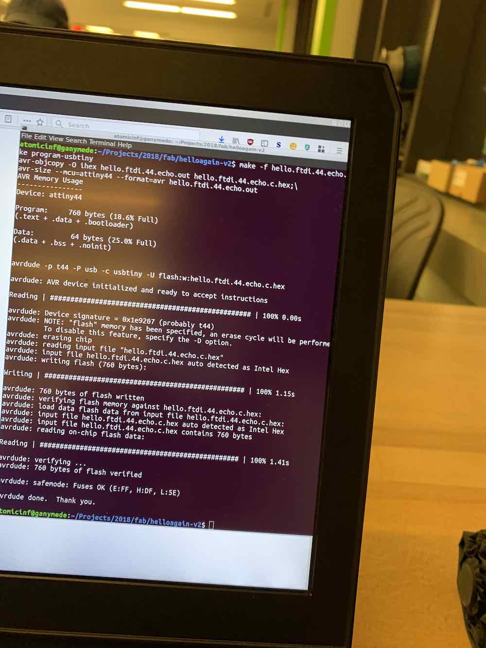
step 7:
i wish i had more information about how to program a board (and i hear that we will be learning how to do that in a couple of weeks), but i went to the EECS section to get some help on programming my board. this is where all my problems came out, and i realized an integral step i will never forget again -- to check my milled board for accuracy. the reason my board wasn't working when plugged in was because i had Two locations where the pad was touching a trace, and i didn't even realize there were two. so i solved one, and then tried to program the board, but then had to go through and check again, where i noticed the second problem. a big pain to fix afterwards, so check your board after milling!!

other things i learned:
i didn't realize you could do design checks in eagle, to ensure that the board was laid out correctly and there were no air wires floating anywere.adding labels and names to the eagle schematic makes things A Lot easier when trying to debug and look at the board.